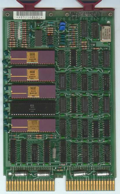
Picture 2: The M7270 module
The LSI-11 was the first microprocessor-based PDP-11 implementation,
introduced in 1975. The processor was the KD11-F, a quad-height
board, which had a few revisions. Although as said, it was microprocessor-based,
the LSI-11 CPU consisted of several chips. The chipset is:
23-00264 Control Chip, 21-11549-00(or -01)
Data
Chip and two Microms: 23-002B5 and 23-001B5. The
remaining socket can be used for the KEV11 option (Extended and
Floating Point Instructions), which is labeled 23-003B5.
The LSI-11/2 was a dual-board version, without on-board memory. Both modules were used in PDP-11/03, PDP-11/03L and embedded systems.
KD11-F: LSI-11
..
Picture 1: The M7264 module
The basic KD11-F modules (M7264-AA, -AB, -BA, -BB, -CB, -DB, -EB, -FB, -HB, -JB) had 8 kB RAM on-board, the later M7264-YA, -YB and -YC versions didn't. The layout was also altered during these revisions. The CPU had a 64kByte (32kWord) addressing limit, ROMs for console ODT, but no bootstraps (which were supplied to PDP-11/03 systems via the TEV11 terminator/bootstrap modules, i.e. you also need that module to have a working system). The console can be accessed via a DLV11 SLU (Serial Line Unit) at CSR 177650 , there's no on-board serial port.
Jumpers on the module:
W1: resident memory bank 1 selected/not selected
W2: resident memory bank 0 selected/not selected
W3: LTC interrupt enabled/disabled
W4: processor-controlled memory refresh on/off
W5: power-up mode bit 0 \
W6: power-up mode bit 1 - if 0 and 1: ODT, if 1 and 0, PC at
173000 (user bootstrap)
W7: -
W7: voltage select, DO NOT CHANGE
W8: -
W9: enable/disable reply from local memory
W10:enable/disable reply from resident memory during refresh
W11:enable/disable on-board memory select
There was a WCS (Writeable Control Store) option of the LSI-11 called KUV11, which was another quad-height module (M8018), connected to the CPU with a ribbon cable which goes into the KEV11 option socket.
Picture 2: The M7270 module
This was a cost-effective version of the original LSI-11, with lower power consuption.
Jumpers on the module:
W1: Master clock enable (DO NOT REMOVE)
W2: -
W3: LTC interrupt enabled
W4: -
W5: power-up mode bit 0 \
W6: power-up mode bit 1 - if 0 and 1: ODT, if 1 and 0,
PC at 173000 (user bootstrap)
W7: -
W8: -
W9: -
W10:-
W11:-
Back to the top
Back to "Qbus modules"
Full Table of Contents
Back to the main page
| Created by: Ákos Varga | Last modified: |